← Mercury 14 Pin Wiring Harness – The Boater’s Lifesaver! Mercury outboard wiring harness diagram 2008 Chevy Silverado Radio Wiring—Sound Upgrade Fast! 2005 chevy silverado wiring diagram radio →
If you are searching about DDR, DDR2 and DDR3 – PCB layout examples you've visit to the right page. We have 25 Pictures about DDR, DDR2 and DDR3 – PCB layout examples like What Does a High Speed PCB Design Mean – Hillman Curtis: Printed, High Speed Pcb Design and Layout, Expert PCB Design Service [ With Step and also RF PCB Design: A Practical Guide for Engineers | Viasion. Read more:
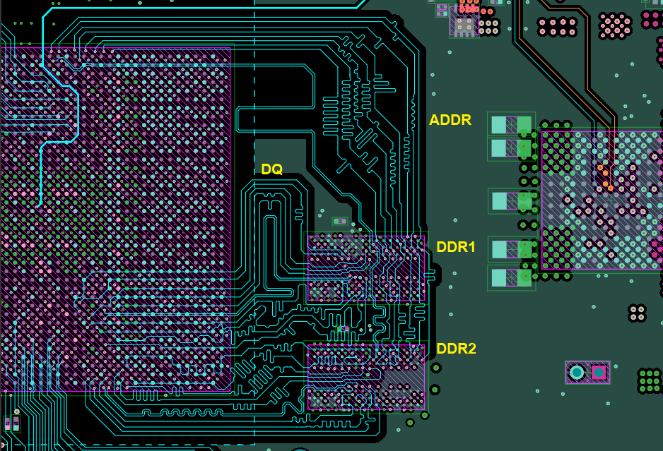
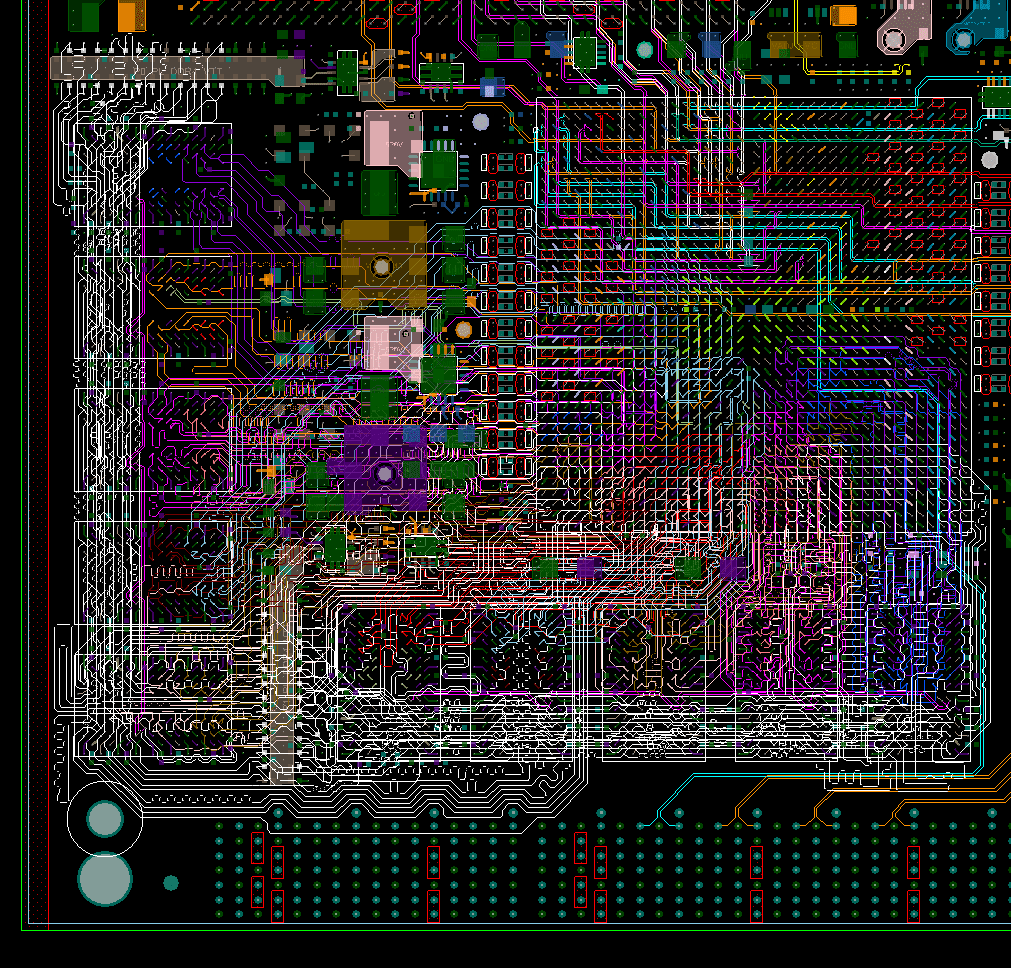
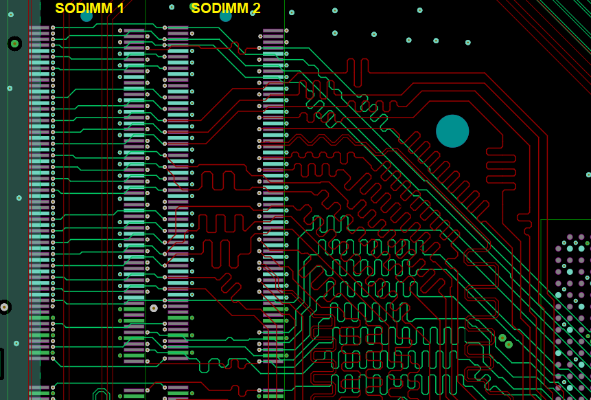
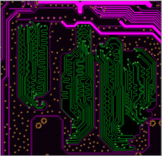
DDR, DDR2 And DDR3 – PCB Layout Examples
 www.fedevel.com
DDR, DDR2 and DDR3 – PCB layout examples
RF PCB Design: A Practical Guide For Engineers | Viasion
 www.viasion.com
RF PCB Design: A Practical Guide for Engineers | Viasion
What Does A High Speed PCB Design Mean – Hillman Curtis: Printed
 hillmancurtis.com
What Does a High Speed PCB Design Mean – Hillman Curtis: Printed ...
LPDDR4 PCB Layout Guidelines | Zuken EN
 www.zuken.com
LPDDR4 PCB Layout Guidelines | Zuken EN
11 Best High-Speed PCB Routing Practices – PCB HERO
 www.pcb-hero.com
11 Best High-Speed PCB Routing Practices – PCB HERO
PCB Layout Guidelines And Considerations
 www.microcontrollertips.com
PCB layout guidelines and considerations
What Is Multi-board Design? | Getting Started | Altium Designer
 resources.altium.com
What is Multi-board Design? | Getting Started | Altium Designer
High Speed Pcb Layout Guidelines - Design Talk
 design.udlvirtual.edu.pe
High Speed Pcb Layout Guidelines - Design Talk
High Speed Pcb Design And Layout, Expert PCB Design Service [ With Step
 www.venture-mfg.com
High Speed Pcb Design and Layout, Expert PCB Design Service [ With Step ...
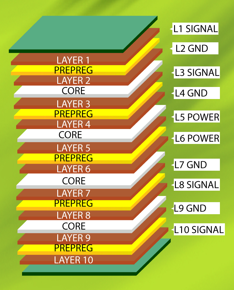
PCB Stack-up: Plan, Design, Manufacture & Repeat | Sierra Circuits
 www.protoexpress.com
PCB Stack-up: Plan, Design, Manufacture & Repeat | Sierra Circuits
Navigate DDR3 PCBs: The Guide For Understanding
 www.venture-mfg.com
Navigate DDR3 PCBs: The Guide for Understanding
Spotting DDR4 Impedance Violations In High Speed PCB Design | Blogs
 resources.altium.com
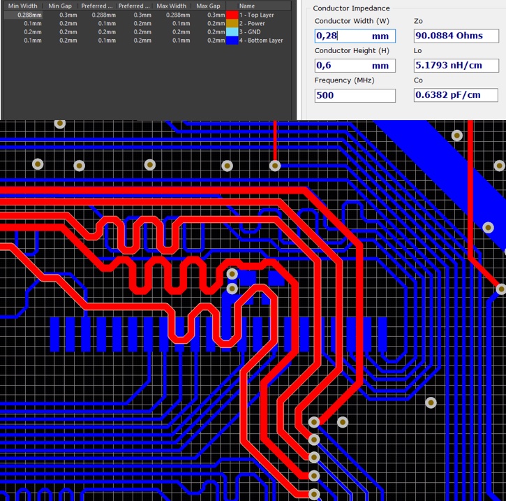
Spotting DDR4 Impedance Violations in High Speed PCB Design | Blogs ...
PCB Schematic And Layout: A Comprehensive Guide – Hillman Curtis
 hillmancurtis.com
PCB Schematic and Layout: A Comprehensive Guide – Hillman Curtis ...
Main Design Guidelines & Layout Rules On High Speed PCB
 www.integrasources.com
Main Design Guidelines & Layout Rules on High Speed PCB
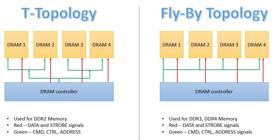
High Speed Designs - Part 9 (T-Topology Vs Fly-By Topology)
 embeddeddesignblog.blogspot.com
High Speed Designs - Part 9 (T-Topology vs Fly-By Topology)
Inspirasi Pcb Routing, Skema Pcb
 skemadriver.blogspot.com
Inspirasi Pcb Routing, Skema Pcb
PCB Routing Guidelines For DDR4 Memory Devices And Impedance | Blog
 resources.altium.com
PCB Routing Guidelines for DDR4 Memory Devices and Impedance | Blog ...
Pcb Routing Guidelines - Design Talk
 design.udlvirtual.edu.pe
Pcb Routing Guidelines - Design Talk
Pcb Trace Width Calculation - Lasopadesignstudio
 lasopadesignstudio743.weebly.com
Pcb trace width calculation - lasopadesignstudio
PCB Design Guidelines For EMI EMC - RayMing PCB
 www.raypcb.com
PCB Design Guidelines For EMI EMC - RayMing PCB
Nine Dot Connects » DDR3, DDR4, LPDDR4 Design And Layout Services, Nine
 www.ninedotconnects.com
Nine Dot Connects » DDR3, DDR4, LPDDR4 Design and Layout Services, Nine ...
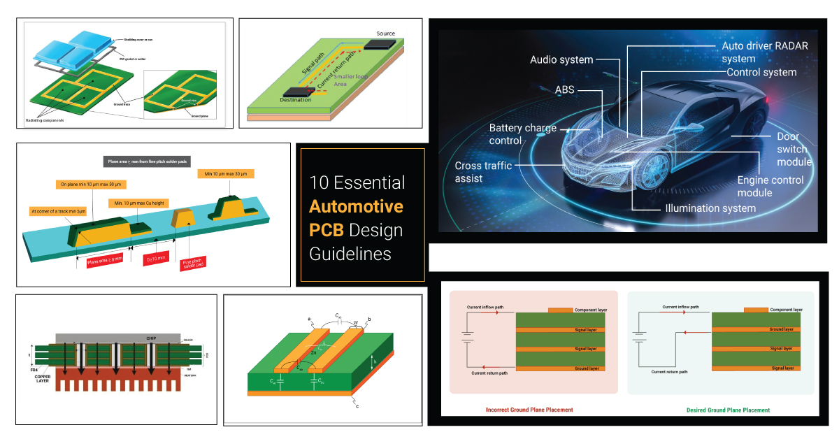
10 Automotive PCB Design Guidelines | Sierra Circuits
 www.protoexpress.com
10 Automotive PCB Design Guidelines | Sierra Circuits
PCB Design & Layout - PCB Design & Engineering Services
 www.freedomcad.com
PCB Design & Layout - PCB Design & Engineering Services
PCB Routing Guidelines For DDR4 Memory Devices And Impedance | Blog
 resources.altium.com
PCB Routing Guidelines for DDR4 Memory Devices and Impedance | Blog ...
Layout Automation And Simulation Reap The Benefits Of DDR4
 www.techdesignforums.com
Layout automation and simulation reap the benefits of DDR4
Pcb stack-up: plan, design, manufacture & repeat. Spotting ddr4 impedance violations in high speed pcb design. pcb design & layout